ASML locks in TSMC, Samsung and Intel for High-NA EUV lithography
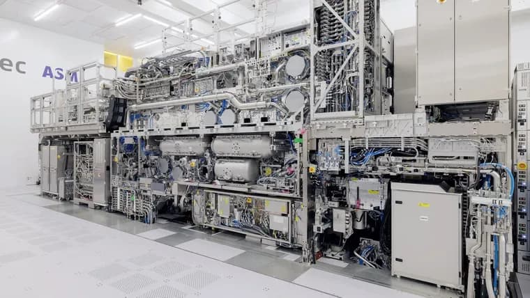
ASML has secured commitments from the world's three leading chipmakers to adopt its newest lithography technology, according to a Bloomberg report. Samsung plans to bring ASML's High-NA EUV machines into high-volume manufacturing starting in 2028, and TSMC in 2030. Intel already has the machines running. A single High-NA EUV unit costs up to $400 million. ASML is the only maker of EUV lithography systems, the equipment needed to print the most advanced AI chips; it brought the simpler Low-NA version to market in 2019 and has since worked with customers to roll out the more complex High-NA machines.
The new deal rests on a shift in photomask size. TSMC, Samsung, Intel and ASML plan to move from today's six-inch photomask standard to twelve inches. A photomask is the stencil that carries a chip's circuit pattern; light passes through it onto a silicon wafer to transfer that pattern, and a bigger mask images more area in a single exposure. The six-inch limit had capped chip size and forced manufacturers to stack chips vertically with complex connections, adding cost. ASML technology chief Marco Pieters said the coordinated push to twelve-inch masks could raise High-NA throughput by 40 percent and called it a huge opportunity. TSMC and ASML plan to build a test line for twelve-inch masks by 2031, with production use on High-NA tools set for 2033.
TSMC had previously held back, arguing the productivity gains from bigger masks did not yet justify the higher cost, but the company is now reversing course. That matters to ASML because TSMC accounts for about 16 percent of its revenue. Samsung, one of the largest memory makers, plans to use High-NA for memory chips starting in 2028, chips whose prices are climbing sharply on demand from AI data centers.
Separately, according to a Financial Times report, Huawei is pushing to strip foreign technology out of China's semiconductor supply chain and work around Western export controls on ASML's technology. Huawei is investing across the lithography chain and helping broker deals with fabs including SMIC. China's effort centers not on EUV but on DUV (Deep Ultraviolet, a 193-nanometer wavelength, versus EUV's 13.5 nanometers); DUV is older and less precise but, using multi-patterning, can still produce more advanced chips at higher cost and effort. At the center of the push is Yuliangsheng, a Shanghai equipment maker that helped develop China's first advanced DUV machine and aims to produce twelve DUV machines by the end of the year. Yuliangsheng was spun out of SiCarrier, which the FT says has close ties to Huawei, a claim Huawei denies. The machine is being tested by SMIC and on Huawei's own production lines, so far only for less complex semiconductors, and Yuliangsheng remains far behind ASML.
Bernstein analyst Lin Qingyuan said Huawei plays a project management role in China's DUV push and that a prototype alone is not enough; thousands of suppliers and customers need to work together under a central orchestrating force. The biggest remaining bottlenecks are projection lenses and light sources. Yuliangsheng uses lenses from Zeiss; it is unclear from the source whether the claim that it sells its optics only to ASML refers to Zeiss or to Yuliangsheng, though insiders point to a secondary market. Huawei's venture capital arm, Habo, is meanwhile backing Zeiss rivals such as Fujian Zhiqi Photonics and light-source developer Beijing RSLaser.
Key facts
- Samsung plans High-NA EUV high-volume manufacturing from 2028 and TSMC from 2030; Intel already runs the machines, each costing up to $400 million.
- The four companies plan to move photomasks from six inches to twelve, a shift ASML's Marco Pieters says could raise High-NA throughput by 40 percent, with a test line targeted for 2031 and production use by 2033.
- TSMC, which accounts for about 16 percent of ASML's revenue, reversed its earlier stance that the productivity gains did not justify the cost.
- Huawei is orchestrating a Chinese push to build domestic DUV lithography around Shanghai maker Yuliangsheng, which aims to produce twelve DUV machines this year and was spun out of SiCarrier, a company the FT ties to Huawei and Huawei denies.
- Bernstein analyst Lin Qingyuan says the effort still faces bottlenecks in projection lenses and light sources, sourced partly from Zeiss, while Huawei's venture arm Habo backs Zeiss rivals.
Why it matters
EUV lithography is the single biggest bottleneck in building advanced AI chips, and ASML is its only maker. Getting TSMC, Samsung and Intel to commit to High-NA on a shared timeline, and to the costly twelve-inch photomask transition, locks in the production roadmap for the chips behind AI accelerators for years. At the same time, Huawei's DUV push shows China trying to route around that single point of dependency under export controls, using an older, less capable technology stretched further through multi-patterning.
Who it affects
TSMC, Samsung and Intel, whose chip roadmaps now depend on ASML's twelve-inch mask timeline; ASML itself, whose revenue leans heavily on TSMC; Samsung's memory business, already under pressure from AI-driven demand; and on the Chinese side, SMIC, Yuliangsheng, SiCarrier, Zeiss and Huawei's venture arm Habo, all pulled into the effort to build a domestic lithography supply chain.
How to use it
There is no product or price here to act on directly. The dates are the useful markers: 2028 for Samsung's High-NA rollout, 2030 for TSMC's, 2031 for the twelve-inch test line, and 2033 for production use of twelve-inch masks on High-NA tools. Anyone tracking AI chip supply, memory pricing, or China's semiconductor self-sufficiency has concrete milestones to watch rather than vague direction.
How solid is it
The ASML side is sourced to a Bloomberg report and includes an on-record quote from ASML technology chief Marco Pieters. The Huawei side is sourced to the Financial Times and includes a named Bernstein analyst, Lin Qingyuan. Neither report is disputed on its main facts, but one link in the chain is explicitly contested: the FT's claim that SiCarrier has close ties to Huawei, which Huawei denies.
Risks and caveats
The twelve-inch mask transition is years out and unproven at scale; TSMC only recently dropped its objection that the costs did not justify the gains. On the Chinese side, Yuliangsheng is described as far behind ASML and so far tested only on less complex chips, and its ties to SiCarrier and Huawei are disputed rather than confirmed. The claim that a secondary market supplies Zeiss lenses comes from unnamed insiders, and it is unclear from the source whether the statement that optics go only to ASML refers to Zeiss or to Yuliangsheng.