LTT Labs CT scans a delidded Intel Core i9-14900KS
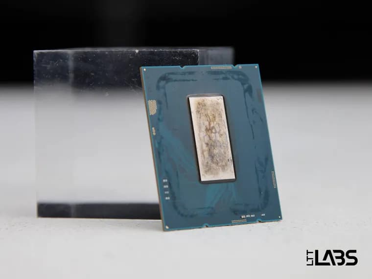
LTT Labs delidded an Intel Core i9-14900KS for an unrelated project and used the opportunity to put it through a CT (computed tomography) scan on the lab's Lumafield Neptune scanner, the same machine it used two years earlier to scan an Intel Core i9-13900K. The scan ran on the 120 kV Neptune unit for 720 minutes, 12 hours, with a 2.5 mm copper filter used to harden the X-ray beam; the resulting scan is published as an interactive model that readers can explore directly through Lumafield's Voyager viewer. On the rear of the CPU's PCB, the scan shows a cluster of capacitors that support the silicon circuitry. LTT Labs explains that the motherboard's own voltage regulation modules (VRMs) sit physically too far from the transistors to fully smooth sudden power draw on their own; the capacitors on the back of the PCB, along with others built directly into the silicon die itself, supply the energy needed for higher-frequency, faster power spikes that the VRMs cannot react to in time. Slicing through the scan layer by layer, the team differentiated three separate PCB layers along with the internal vias connecting them. In the same slices they say they can also make out what they believe is part of the silicon's internal structure, though the dense capacitor components sitting beneath the silicon introduce scan noise; LTT Labs notes that this noise pattern looks visually distinct from the actual silicon patterns, which is how they distinguish the two. Comparing the CT capture against the chip's known die layout, the team identifies the E-cores and P-cores, with a horizontal band running down the center of the die housing cache and the internal bus, and the integrated GPU, media engines and supporting circuitry populating the left and right sides.
Key facts
- LTT Labs CT scanned a delidded Intel Core i9-14900KS on a Lumafield Neptune scanner, following an earlier scan of an i9-13900K two years before.
- The scan used the 120 kV Neptune unit for a 720-minute (12-hour) duration with a 2.5 mm copper filter to harden the X-ray beam.
- Rear-PCB capacitors, and others built directly into the silicon die, supply power for fast, high-frequency spikes because the motherboard's VRMs sit too far from the transistors to react in time.
- The scan differentiated three PCB layers plus internal vias, and captured what LTT Labs believes is part of the silicon's internal structure despite noise from nearby capacitors.
- Comparing the scan to the known die layout, the team identifies the E-cores and P-cores, a central cache/bus band, and the integrated GPU and media engines on either side.
Why it matters
CT scanning is one of the few ways to see inside an assembled CPU package without physically cutting it apart and destroying the very structure you want to examine. Applied here to a mainstream desktop chip, it turns an otherwise opaque piece of silicon and PCB into something a reader can visually inspect layer by layer, matching capacitor placement, PCB routing and even rough die structure to what is normally only described in datasheets or block diagrams.
Who it affects
This is aimed at PC hardware enthusiasts, overclockers and CT/imaging hobbyists who follow LTT Labs' teardown work, rather than at buyers of the i9-14900KS itself; nothing here changes how the chip performs or should be used.
How to use it
The scan LTT Labs produced is published as an interactive 3D model that can be explored directly in Lumafield's Voyager viewer, letting readers rotate, slice and zoom into the CT data themselves rather than relying only on the still images in the writeup.
How solid is it
The material is LTT Labs' own first-person account of a scan it ran itself, published without a named individual author or a specific date beyond describing the earlier i9-13900K scan as roughly two years prior; the settings (voltage, duration, filter) are stated precisely, but the structural claims (which patterns are silicon versus scan noise, which regions are which core type) are the lab's own visual interpretation of the imaging rather than independently confirmed measurements.
Risks and caveats
LTT Labs itself flags that dense capacitor components beneath the silicon introduce CT scan noise, and that distinguishing this noise from genuine silicon structure relies on the patterns looking visually distinct rather than on a verified separation method. The writeup includes no performance, temperature or benchmark data, no die size or transistor count, and does not name or describe the unrelated project that led to the chip being delidded in the first place.
“We've been able to differentiate three PCB layers as well as the internal vias.”
— LTT Labs