AMD explains why EPYC Venice uses 2.5D packaging and two I/O dies
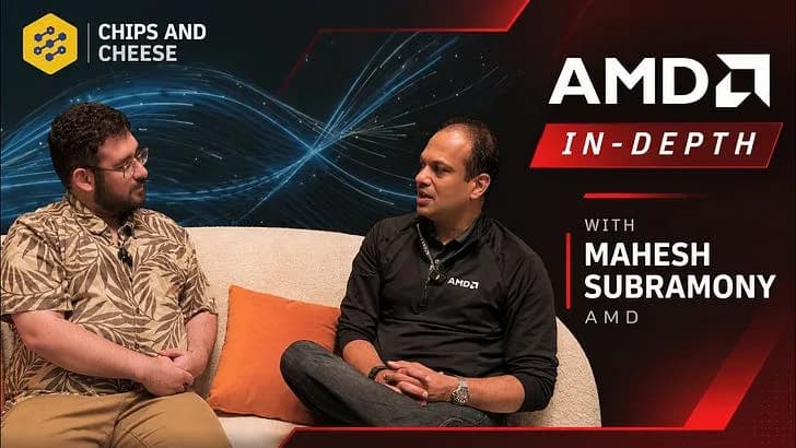
Chips and Cheese published an edited transcript of George Cozma's conversation with AMD's Mahesh Subramony, recorded at AMD In-Depth, about the SoC design of the new EPYC Venice processors (Zen 6). Subramony says his role has changed since their last talk: he is now a corporate vice president of design engineering and leads server architecture.
The starting point is bandwidth. Cozma notes that Venice is AMD's first server CPU with 2.5D packaging. Subramony says the previous generation moved a little under 700 GB/s between the CPU chiplets and the I/O die (he prefaces this with "I think"), and that standard packaging with the older GMI links made sense at that level. Venice moves 1.6 TB/s, with each CCD overprovisioned as it drives data into the I/O die. His estimate is that moving that much data over conventional packaging would have eaten roughly 10 to 15% of the overall SoC power budget, whatever picojoules-per-bit figures appear in papers. Advanced packaging gives a low-power, high-bandwidth, low-latency link instead.
The catch is geometry. Very short die-to-die connections mean the dies must match widths at the interface, keep the link to a handful of millimetres, and offer enough perimeter and "beachfront" for the CCD connections as well as for the I/O. In earlier generations the links could take long routes through the package. Subramony calls these constraints one of the foundational reasons AMD split the I/O into two dies, and says the fast package link meant the split did not burden power or latency much.
AMD uses the same I/O die design twice, with one copy rotated 180 degrees, instead of building two distinct dies. The cost is some area overhead, because one-off blocks such as the root of trust and boot I/O get duplicated. The harder part was fabric topology: in an NPS1 configuration the two dies must act as one domain, and delivering the right quality of service, bandwidth and latency with the mirrored design was a challenge. Subramony adds that he thinks tiled approaches will become increasingly advantageous as core counts grow.
SP7 and SP8 do not share an I/O die. The enterprise market behind SP8 had lower compute requirements and cost sensitivity, the overhead in the SP7 I/O dies did not carry over well, and SP8 needed many I/O lanes where SP7 focused on compute and memory bandwidth. A single superset die would have added cost to both, so AMD built two designs. The SP7 die is built for more compute, fewer I/O lanes and more memory channels. SP8 has half as many memory channels, all 128 PCIe lanes per socket, and targets up to 96 cores on the Zen 6 side and 128 on the Zen 6c side.
On the CCDs, the 12-core CCD has three links to the I/O die and the 32-core CCD has four. The four SDP ports on the 32-core design follow roughly one port per eight cores. The 12-core CCD is paired with MRDIMMs and has to draw much more bandwidth per core to saturate 16 channels of 12,800 MT/s MRDIMMs, so three ports can look excessive per core, but the aim is for each CCD to help saturate the SoC's memory bandwidth.
The 32-core CCD physically has 33 cores and 33 L3 slices. As CCDs grow, defects hurt yield more, and AMD found it could fit a 33rd core; the design can harvest any one core and its cache slice while keeping the mesh intact. Active cores are always 32, and Subramony says there will not be a product with 33 active cores, which keeps cache associativity and mesh topology relatively simple.
Cozma asks about latency between the two CCDs. Subramony says a larger L3 takes longer to decide a hit or miss, so the 128 MB L3 costs a few extra clocks before a request goes farther out; the rest of the path from fabric to memory is almost identical. AMD believes the extra capacity more than balances this in workloads that benefit, since more hits, especially with more resident threads on the CCD, are far faster than going to memory. On an otherwise idle CPU with a closed-page DRAM load, a latency difference between the two CCDs will show, largely from the L3 lookup.
Finally, Cozma asks whether the dense CCD could get 3D V-Cache, for something like 384 MB of L3 on one CCD. Subramony points to the 96-core offering, where a 12-core CCD with X3D adds 96 MB of L3 for about 144 MB per CCD. For the dense CCD he calls stacked cache expensive and not a current focus: the 256-core part is meant for balanced throughput under a very tight per-core power budget, and AMD would look at more bandwidth or frequency first. The interview ends with a running joke about cheese.
Key facts
- Venice moves 1.6 TB/s between CPU chiplets and the I/O die, versus a little under 700 GB/s in the previous generation as Subramony recalls it.
- Subramony estimates conventional packaging would have spent roughly 10 to 15% of the SoC power budget just moving those bits, which is why AMD went to 2.5D packaging.
- The I/O is split into two dies using one design, with one copy rotated 180 degrees; the cost is some area overhead from duplicated one-off blocks.
- SP7 and SP8 get different I/O dies: SP8 has half as many memory channels, 128 PCIe lanes per socket, and up to 96 Zen 6 or 128 Zen 6c cores.
- The 32-core CCD physically has 33 cores for yield, but active cores are always 32, and its 128 MB L3 adds a few extra clocks of lookup latency.
Why it matters
The interview gives a first-hand engineering rationale for a big shift in AMD's server design. Cozma describes Venice as AMD's first server CPU with 2.5D packaging. According to Subramony, the driver is raw data movement: 1.6 TB/s between chiplets and I/O die is too much to move over conventional packaging without spending an estimated 10 to 15% of the SoC power budget. The same packaging constraints then shaped the I/O die itself, leading to the two-die split.
Who it affects
Mainly people who follow or plan around AMD's server platforms: SP7 is aimed at more compute and memory bandwidth, SP8 at the enterprise market with lower compute needs and more I/O lanes. Anyone comparing the 12-core and 32-core CCD variants, or the 96-core and 256-core parts, gets the reasoning behind their different link counts, L3 sizes and cache plans.
How to use it
Treat it as a guide for reading Venice specifications. The 12-core CCD parts are designed to be paired with MRDIMMs and to saturate 16 channels of 12,800 MT/s, which is why they have three links per CCD. SP8 trades memory channels for all 128 PCIe lanes per socket. When measuring, expect the larger CCD's L3 lookup to add a few clocks in idle, closed-page DRAM tests, and judge it by effective workload latency, as Subramony suggests. Do not expect a 33-active-core product.
How solid is it
This is an edited transcript of an interview with the AMD executive who leads server architecture, so the design rationale comes from the source. The transcript was edited for readability and conciseness. No measured benchmark or latency number is given; the L3 penalty is only "a few extra clocks". The 10 to 15% power figure is a hypothetical for conventional packaging, not a measurement of Venice, and the previous-generation 700 GB/s figure is recalled with "I think".
Risks and caveats
Much of the benefit is stated as AMD's belief: the company says the extra L3 capacity more than balances the added lookup latency in workloads that benefit, and that splitting the I/O die did not burden power or latency much. The tiled-design outlook is an opinion hedged with "I think". The mirrored I/O design carries area overhead and a topology challenge in NPS1. A 3D V-Cache die on the dense CCD is called expensive and not a current focus, so larger cache on the 256-core part should not be assumed.
“There won’t be a product with 33 active cores.”
— Mahesh Subramony, AMD, in an interview with Chips and Cheese