Samsung's LPDDR5X-PIM does math inside DRAM, software isn't ready
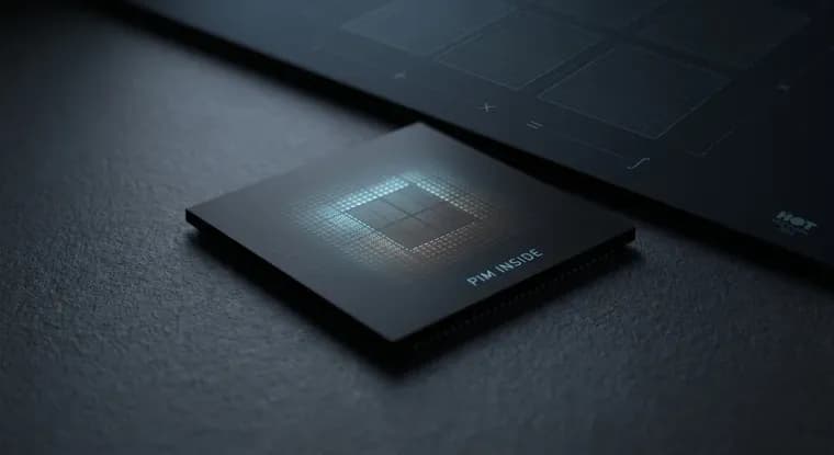
At Hot Chips 2026, Samsung presented a 16 GB LPDDR5X memory package, called LPDDR5X-PIM, that puts compute units inside the memory die itself rather than only behind the usual pins. The chip delivers 614 GB/s of bandwidth to its own compute units directly from the DRAM banks, against just 76.8 GB/s that reaches the outside world through the package's external pins, an eightfold gap reported by Tom's Hardware. That gap is the whole argument for processing-in-memory (PIM): DRAM banks already carry far more bandwidth internally than the external interface can expose, so moving compute next to the banks lets a chip use bandwidth that otherwise goes to waste.
The scale of that number: 614 GB/s matches the total memory bandwidth of Apple's top-spec M5 Max, the 40-core GPU configuration in the $3,499 MacBook Pro, drawn across its entire unified memory system. Samsung reaches the same figure from inside a single memory package. Apple's own chip lineup shows why bandwidth matters so much for local inference: the M5 Pro moves 307 GB/s, the M5 Max moves 460 or 614 GB/s depending on configuration, and the M5 Ultra reaches 1.2 TB/s, and those numbers predict local tokens per second better than TFLOPs do, since Apple pays for a wide external interface to get there. Author Ben Houston frames the underlying problem with a simple model: generating one token means reading every parameter from DRAM once, multiplying it, and discarding it, so tokens per second is roughly memory bandwidth in GB/s divided by model size in GB. At 614 GB/s against a 20 GB model, that puts the hard ceiling around 30 tokens per second, and the real figure runs lower still because the KV cache grows with context and competes for the same bandwidth.
Physically, Samsung's package places sixteen PIM compute blocks beside the DRAM banks, with MAC trees running in parallel and an ALU for floating-point and integer math, inside a JEDEC-standard 561-ball part holding 16 GB across four dies per rank. It processes data in four steps: an activation write broadcasts FP8 activation data into the banks, a weight load reads 32-byte weight elements from DRAM cells and maps them across the MAC trees, a vector store writes partial sums back to the bank, and a readback step switches to single-bank mode to drain the 1-kbit vector register file in up to 64 sequential reads. Weights never leave the package; only the far smaller activations cross the bus. The part supports fifteen precision combinations, reaching 2.4 TOPS with SINT4 weights and about 1.2 TFLOPS with FP8, and Samsung's Address Align Mode lets a conventional memory controller drive it without requiring every SoC vendor to design a new one, which the article treats as the difference between PIM shipping and PIM staying a research prototype.
Samsung validated the design on real silicon in its own edge AI accelerator SoC, comparing plain LPDDR5X against LPDDR5X-PIM while running Llama 3.1 8B at a 320-token context with SINT8 activations, SINT4 weights, and SINT32 output. Houston is explicit that this is a vendor benchmark covering one model, one short context, one accelerator, and integer quantization throughout: it shows the architecture works on silicon, not that it will perform well on every workload, and the short 320-token context in particular keeps the KV-cache problem out of the picture. Samsung has not disclosed package pricing, so the cost case against a wider, HBM-style memory interface remains a claim rather than a measured result. The commercial motive is clear regardless: memory's share of AI chip component spending rose from 52% in Q1 2024 to 63% by Q4 2025, mostly driven by HBM, and Samsung has chased a cheaper route to HBM-class bandwidth since its Aquabolt-XL HBM2-PIM proof of concept in 2021; LPDDR5X-PIM is its first LPDDR-based PIM design to reach productization.
None of that reaches a developer's machine yet. No PIM backend exists in llama.cpp, vLLM, or any other mainstream inference runtime; Samsung offers only a simulator, a datasheet on request, and an SDK with reference tooling. Houston lists three concrete obstacles. First, llama.cpp's GGUF k-quant formats such as Q4_K_M rely on per-block and per-superblock scaling that needs general-purpose logic PIM's minimal MAC units have no room for (one cited alternative design paid about 126% area overhead just to add FP16 and INT32 support), so existing quantized model files would need re-quantizing into a PIM-native layout, with an unknown quality cost. Second, PIM needs its weight matrix laid out contiguously and bank-aligned, but macOS, Linux, and Windows provide no huge-page-backed, bank-aware allocator today, which conflicts with the memory-mapped model loading that makes llama.cpp convenient to use. Third, bank-level PIM designs, Samsung's included, are built for GEMV, the matrix-vector math of single-batch decoding, while prefill, batched serving, grouped-query attention, and speculative decoding all push work toward GEMM, where PIM's bank-level throughput cannot fully engage. Samsung's current design also stops its NPU from touching DRAM whenever PIM is active, so the two processors cannot split a single layer's work between them.
The article weighs PIM against multi-token prediction (MTP), the technique Google reports delivering up to a 3x speedup with Gemma 4 by having extra prediction modules draft tokens for the main model to verify in parallel. MTP and PIM both cut the cost of reading model weights, MTP by amortizing one read across several accepted tokens, PIM by making each remaining read faster, so their gains would not simply add up, and on hardware available today MTP may be the larger, cheaper win for models with accurate draft heads. Mixture-of-experts routing adds a further complication: if a model's active experts sit on a subset of banks, some banks run hot while others idle, undermining PIM's advantage. Researchers have proposed several fixes, from splitting prefill and decode between an NPU and PIM (AttAcc, IANUS, NeuPIMs) to putting real GEMM units on an HBM logic die (Duplex, which fits 32 GEMM modules with 512 FP16 MACs each into 17.80 mm², about 14.7% of a 121 mm² HBM3 die) to building heterogeneous compute directly into memory (CENT, HALO). Samsung's own choice, near-bank compute in a JEDEC-standard package with a conventional controller, trades some of that flexibility for something that can actually ship in familiar hardware today.
Key facts
- Samsung's 16 GB LPDDR5X-PIM package delivers 614 GB/s of internal bank-level bandwidth versus 76.8 GB/s through its external pins, an eightfold gap reported by Tom's Hardware.
- That 614 GB/s matches the total bandwidth of Apple's top-spec M5 Max (40-core GPU, $3,499 MacBook Pro), but Samsung produces it from inside one memory package rather than a wide external interface.
- Samsung validated the chip on Llama 3.1 8B at a 320-token context with SINT8 activations, SINT4 weights, and SINT32 output, on its own edge AI accelerator SoC; it has not disclosed package pricing.
- Memory's share of AI chip component spending rose from 52% in Q1 2024 to 63% by Q4 2025, mostly HBM, which is why a cheaper route to HBM-class bandwidth matters to vendors.
- No PIM backend exists in llama.cpp, vLLM, or any mainstream runtime: GGUF k-quant formats don't map to the hardware, no OS provides the bank-aware allocator PIM needs, and the design favors GEMV over the GEMM used in prefill, batching, and speculative decoding.
Why it matters
Local LLM inference is bottlenecked by memory bandwidth, not compute: generating each token means reading every model parameter from DRAM once and discarding it, so tokens per second tracks bandwidth divided by model size far more than it tracks TFLOPs. LPDDR5X-PIM attacks that bottleneck directly by putting compute units inside the DRAM die, next to the banks, so it can use the 614 GB/s of internal bandwidth those banks already have instead of squeezing everything through 76.8 GB/s of external pins. It ships in a JEDEC-standard 561-ball package that a conventional memory controller can drive, which is what makes it a product rather than a lab curiosity: Samsung has chased this idea since its Aquabolt-XL HBM2-PIM proof of concept in 2021, and this is its first LPDDR-based PIM design to reach productization. The pitch to the industry is HBM-class inference bandwidth without HBM's price, power draw, or packaging complexity, at a moment when memory has grown from 52% to 63% of AI chip component spending in two years.
Who it affects
SoC and device vendors building local-inference hardware for phones, laptops, and servers are the direct audience, since Address Align Mode lets them adopt PIM without a new memory controller. Edge AI accelerator designers get Samsung's own validated reference point (the Llama 3.1 8B benchmark). Runtime maintainers, llama.cpp, vLLM, and anyone shipping GGUF-quantized models, are the ones who would have to build support that does not exist today. Competing memory vendors, including SK hynix with its own GDDR6-PIM, work the same near-bank-compute angle. End users hoping for faster on-device LLM inference are the eventual beneficiaries, but only once the software layers below catch up.
How to use it
Nothing here is usable yet. Samsung has not disclosed package pricing or given a shipping timeline, and no mainstream inference runtime has a PIM backend. What is available to developers today is a simulator, a datasheet on request, and an SDK with reference tooling, aimed at experimentation rather than deployment. Turning that into a working stack means re-quantizing models into a PIM-native layout, since Samsung's fifteen supported precision modes (up to 2.4 TOPS at SINT4, about 1.2 TFLOPS at FP8) do not include the k-quant formats llama.cpp relies on.
How solid is it
This is real silicon, not a paper design: Samsung ran the comparison on its own edge AI accelerator SoC, measuring plain LPDDR5X against LPDDR5X-PIM. But it is also, in the article's own framing, a vendor benchmark covering exactly one model (Llama 3.1 8B), one short 320-token context, one accelerator, and integer quantization throughout, which demonstrates that the architecture works on silicon without predicting performance on other workloads. The short context in particular keeps the KV-cache growth problem out of the result. The oft-cited ~30 tokens/second figure is the article's own back-of-envelope ceiling from a bandwidth-over-model-size formula, not a number Samsung measured, and it is explicitly described as an upper bound that the real number falls short of. The cost advantage over a wider memory interface is, by the article's own account, an unverified claim, since no price has been disclosed.
Risks and caveats
Three separate software obstacles stand between this silicon and a working product. GGUF k-quant formats like Q4_K_M need per-block scaling logic that PIM's minimal MAC units have no die area for, so existing quantized models would need re-quantizing with an unknown quality cost. No current operating system provides the huge-page-backed, bank-aware memory allocator PIM needs, and that requirement conflicts with the memory-mapped model loading llama.cpp is built around. And bank-level PIM designs, this one included, are optimized for GEMV, which fits single-batch decoding well but loses effectiveness as batching, grouped-query attention, and speculative decoding push modern inference toward GEMM; Samsung's design also blocks its NPU from accessing DRAM whenever PIM is running, so the two cannot split a layer's work concurrently. Mixture-of-experts routing can leave some memory banks idle while others run hot, further eroding the advantage. Multi-token prediction, a software-only technique already delivering up to 3x speedups on Gemma 4, competes for the same underlying gain (cheaper weight reads), so PIM's real-world benefit will not simply add on top of it.