Samsung shows zHBM stacking memory on AI chips, claims up to 8x performance
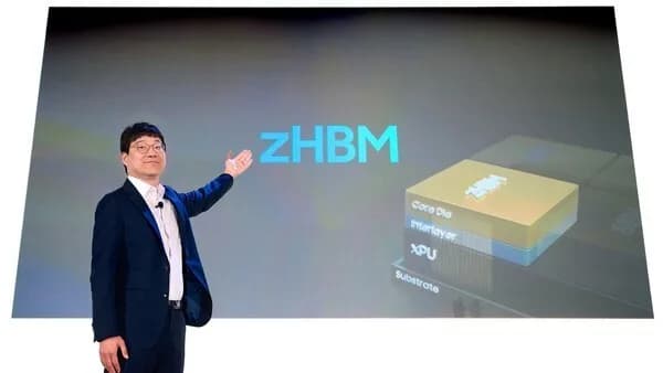
Samsung Electronics showed off two new 3D memory technologies, zHBM and zNAND-O, at the Future of Memory and Storage (FMS) 2026 conference in California, part of a push to strengthen its position in the rapidly growing artificial intelligence market. The company outlined both during a keynote on Aug. 4, then showed physical mockups of each for the first time the next day, Aug. 5.
zHBM (Samsung's name for "z-axis High Bandwidth Memory") is the headline technology: a next-generation architecture that stacks HBM vertically on top of AI accelerators, or xPUs, along the z-axis, rather than placing the memory around the chip as conventional designs do. Samsung says this shortens the distance data has to travel between memory and processor, and that conventional architectures are running into limits meeting the performance demands of next-generation HPC and AI infrastructure. The company claims zHBM can deliver up to eight times the data-processing performance of its eighth-generation High Bandwidth Memory (HBM5), triple the performance per watt, and cut thermal resistance by more than half. zHBM is built as a customizable family: customers can add their own semiconductor IP blocks to an interlayer placed between the memory and the accelerator, tailoring the stack for capacity or performance on specific workloads. Samsung says it plans to work closely with customers to co-optimize AI processors and memory systems around zHBM.
Samsung also introduced zNAND-O, a next-generation NAND flash family still under development. It combines Samsung's V-NAND vertical stacking architecture with Through-Silicon Via (TSV) technology, the same kind of interconnect HBM uses to link stacked DRAM dies, giving zNAND-O a structure similar to the High Bandwidth Flash (HBF) that SK Hynix and Sandisk are separately developing. The "O" stands for on-device AI applications. Samsung demonstrated four-layer and eight-layer 3D-packaged V-NAND configurations built for high space efficiency, higher read bandwidth and faster response times, which it says suit workloads needing real-time processing of large data volumes. The zNAND-O mockup on display was built on Samsung's V10 Bonding Vertical (BV)-NAND platform, also unveiled at the keynote, which has more than 400 layers and separates the NAND cell array from its peripheral circuitry onto different wafers before vertically bonding them together; the V-NAND cells themselves are made in three separate stacks and then interconnected vertically. Samsung says this raises memory density by about 58% over the previous V9 generation while also improving read, write and input/output performance.
Samsung's exhibition area carried more than 30 memory products in total. Beyond zHBM and zNAND-O, highlights included a next-generation AI computing platform built on HBM4E, wafer samples, and a separate HBM5 mockup fitted with Heat Path Block (HPB) technology, which adds vertical heat-dissipation channels along the sides of the HBM core dies to improve thermal management. Samsung also showed LPDDR5X-PIM, low-power LPDDR5X DRAM combined with processing-in-memory functionality, which it describes as the world's first implementation of its kind. On the storage side, the company displayed two AI-focused enterprise SSDs: the PM1763, built for high-speed reading and efficient data processing, and the BM1773, an ultra-high-capacity drive for large-scale AI training datasets.
Samsung tied all of it to its own positioning as, in its words, the world's only integrated device manufacturer able to offer memory, logic semiconductors, foundry services and packaging from one source. "We can provide integrated services from the product design stage through mass production, helping customers shorten development cycles while optimizing performance and power efficiency," the company said. "This enables customized AI semiconductor solutions tailored to customer requirements."
Key facts
- Samsung showed mockups of zHBM and zNAND-O for the first time on Aug. 5 at the Future of Memory and Storage (FMS) 2026 conference in California, a day after outlining both in an Aug. 4 keynote.
- zHBM stacks HBM vertically on top of AI accelerators along the z-axis instead of placing memory around the chip; Samsung claims up to eight times the data-processing performance of its eighth-generation HBM5, three times the performance per watt, and less than half the thermal resistance.
- zNAND-O, still under development, combines V-NAND stacking with through-silicon-via (TSV) technology in a structure similar to the High Bandwidth Flash that SK Hynix and Sandisk are separately developing; Samsung showed four-layer and eight-layer 3D-packaged versions.
- Samsung's V10 Bonding Vertical (BV)-NAND has more than 400 layers and, built as three separately manufactured and bonded wafer stacks, raises memory density by about 58% over the previous V9 generation.
- The showcase, which spanned more than 30 memory products, also included LPDDR5X-PIM (low-power DRAM with built-in processing-in-memory, which Samsung calls a world first) and two new enterprise SSDs for AI workloads, the PM1763 and the ultra-high-capacity BM1773.
Why it matters
Samsung's case for zHBM is structural rather than just a faster chip: conventional designs place HBM around the AI accelerator, and the company says that approach is running into limits on the performance next-generation HPC and AI infrastructure needs. Putting memory directly on top of the accelerator along the z-axis is Samsung's fix, meant to shorten the distance data has to travel between memory and processor. The company's own figures, up to eight times the data-processing performance and three times the performance per watt of its eighth-generation HBM5, plus less than half the thermal resistance, describe a large jump if it holds up beyond a trade-show mockup. The zNAND-O and V10 BV-NAND work extends a similar logic, through-silicon vias and wafer bonding, to flash storage: Samsung positions zNAND-O for on-device AI and real-time processing of large data volumes.
Who it affects
The direct audience is AI-accelerator and HPC-chip designers, since Samsung's pitch for zHBM is a customizable interlayer that customers add their own semiconductor IP blocks to, built through co-design with Samsung rather than bought as an off-the-shelf part. It also affects buyers of large-scale AI training and inference infrastructure: the same showcase included the PM1763 and BM1773 enterprise SSDs, the latter aimed at large-scale AI training datasets, plus the LPDDR5X-PIM memory. Samsung ties the whole lineup to its own push to strengthen its position in the rapidly growing AI market, and to its claim of being the only integrated device manufacturer spanning memory, logic semiconductors, foundry services and packaging under one roof.
How to use it
None of this is available to buy yet. The source gives no pricing, no release date and no mass-production timeline for zHBM or zNAND-O; zNAND-O is explicitly described as still under development. zHBM's path to use is co-design: a customer works with Samsung to add its own IP blocks to the interlayer between memory and accelerator, tailored to its workload, and Samsung says it plans to work closely with customers on that co-optimization going forward. No customer is named as having adopted or tested zHBM or zNAND-O yet.
How solid is it
Every figure and claim here is Samsung's own: the article attributes each statement to "Samsung" or "the company," and no individual engineer or executive is named or quoted. What was shown at FMS 2026 were mockups, not shipped hardware or figures benchmarked by an outside party: the source uses the word "mockup" throughout, including for the zHBM and zNAND-O pieces and for a separate HBM5 unit fitted with Heat Path Block cooling. The performance multiples, up to eight times the data-processing performance and three times the performance per watt, are both stated relative to Samsung's own eighth-generation HBM5, and the source gives no absolute baseline numbers for HBM5 itself to check them against; the claimed drop to less than half the thermal resistance carries no stated baseline of its own. The Hacker News discussion this story arrived on drew minimal engagement, six points and two comments, so there has been no real outside scrutiny of the claims yet.
Risks and caveats
Samsung isn't alone chasing this shape of idea: the source says zNAND-O's structure resembles High Bandwidth Flash (HBF), which SK Hynix and Sandisk are separately developing, so Samsung's version is not guaranteed to be the one that becomes standard even if the performance numbers hold up. Demonstrations at a trade show routinely look better than what eventually ships, and every number here is a Samsung-stated multiplier against its own prior generation rather than an independently measured result. The source also does not say that any customer has adopted or is testing zHBM or zNAND-O, only that Samsung plans to work with customers going forward, and it gives no release date for either.
“We can provide integrated services from the product design stage through mass production, helping customers shorten development cycles while optimizing performance and power efficiency. This enables customized AI semiconductor solutions tailored to customer requirements.”
— Samsung